The Mounting Hole: Ensuring Reliable Grounding in PCB Projects
When working with sensitive analog or RF signals, PCB projects need to address both on and off board noise sources. Many times, our PCB solution is only one piece of an integrated, complex solution. As an experienced engineer, I can tell you that dealing with foreseeable issues at the board level is much easier and more cost effective than waiting until system integration. If you think high frequency on a singular PCB is challenging, spend some time trying to track down inductive coupling at the system level. It’s enough to make even a seasoned engineer pull their hair out and at the same time crush a project budget.
A common customer concern that frequently comes up is how, or even if, to effectively ground the electronics to the hardware frame. By implementing a few good PCB housekeeping policies we can make it easier on all involved to tackle the unknown. In situations where customers do not specify grounding requirements, it is advisable to incorporate at least one plated through hole for chassis mounting of your PCB. To do this we should first understand that typical through hole wall plating coverage on Class I (general) and Class II (service) PCBs will be about 0.8mils (20 microns). If doing Class III (military/space) you can expect about a 1mil (25 microns) wall thickness. This wall thickness, in conjunction with screw head pressure due to torquing and sharp thread edges, can leave plenty of opportunity for tearing the plating from pours and/or planes both internally and externally to the PCB. These can cause electrical disconnect.
So the question remains, how do we design for grounding (or not grounding) and at the same time make sure this will be reliable. If we are unsure whether to ground or not, it is in our best interest to make one of our mounting holes a plated through hole and have a connection between it and our external ground pour via a 0 ohm resistor population option. I typically make the connection with a 20 – 50 mil trace width, depending on the resistor package size which in turn depends on the board size, thus keeping inductive impedance low. In more than two layer boards any external ground pours will always be connected to your internal ground plane through vias. If your board is two layers or less one of the external layers should be poured as ground. On the other hand, if the customer is confident they want the PCB directly grounded then the plated through hole can have spoked or direct connect to the appropriately named signal on the pours/planes. This second scenario has an added benefit of allowing for thermal relief of the PCB to the chassis.
With this option in place for the uncertainty we now focus our concern on the reliability of the connection. First, I recommend using washers, either star or flatted. Recall, a flat washer will spread a screw head load across the external copper land helping to protect from tearing due to over-torquing. A star washer will be more effective in maintaining friction between the screw and the PCB in a vibration environment but can cut into the copper land. It is with this information that we will make a choice on which direction we go with the washer.
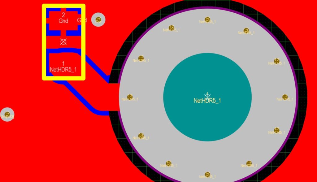
With respect to the PCB, I traditionally create a ring of vias within the land but beyond the edge of the screw head. The above picture is showing a mounting hole for a 6mm screw head. These vias afford me protection from the potential screw thread cutting that can occur on the thinly plated hole wall and create internal copper discontinuity. I have found it unnecessary to place the vias beyond the diameter of the washer even if it is a star. Although the star will cut, it is highly unlikely to shear all the vias.
Ensuring reliable grounding in PCB projects can be a challenging task. However, by implementing the mounting hole PCB technique mentioned above, the assembly of the board into the overall system comes down to population options for the washer and a 0 ohm resistor. These simple yet effective measures contribute to the stability and performance of electronic devices, reducing the potential for interference and improving overall reliability.